BlogGuides
KiCad DRC errors: what each one means and how to fix it
A practical guide to KiCad’s design rule checker: clearance, shorting items, courtyards, starved thermals, solder mask bridges, silkscreen, unconnected items, and parity.
KiCad’s design rule checker compares the board with the rules in Board Setup and any custom rules, and lists every place they disagree. A first run on a real board usually returns hundreds of items, most of them silkscreen. This guide covers what each common violation means, how to fix it, and what order to work in.
Running DRC
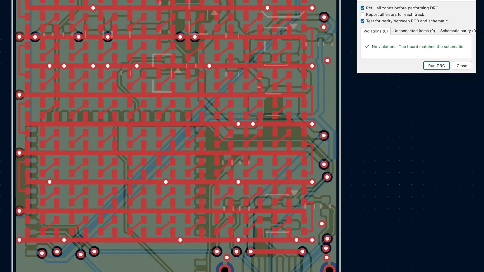
In the PCB Editor, choose Inspect → Design Rules Checker. Turn on Refill all zones before performing DRC and Test for parity between PCB and schematic, then select Run DRC. To run the same check from a script or CI, use the command line:
kicad-cli pcb drc --schematic-parity --refill-zones --severity-all \
  --exit-code-violations --format json -o drc.json board.kicad_pcb
What the common violations mean
| Violation | What it means | Usual fix |
|---|---|---|
| Items shorting two nets | Copper from two different nets touches. | Find the crossing track or overlapping pad and reroute it. Fix these first. |
| Clearance violation | Two items on different nets are closer than the clearance rule. | Move the track, shrink a neck-down, or check whether the net class rule is too strict. |
| Copper edge clearance | Copper is too close to the board outline. | Pull tracks and zones back from the edge, or set the zone’s edge clearance. |
| Courtyards overlap | Two footprints’ courtyard outlines intersect. | Spread the parts. A real overlap means the pick-and-place nozzle or the parts themselves will collide. |
| Starved thermal | A pad connects to a zone through fewer thermal spokes than the rule requires. | Clear space around the pad so the spokes fit, or change the pad’s zone connection. |
| Solder mask bridge | A mask opening joins pads on different nets. | Increase mask expansion clearance, or allow bridging for fine-pitch parts if your fab can’t make the web. |
| Hole clearance | A drilled hole is too close to copper on another net. | Move the via or track away from the hole. |
| Via is not connected | A via connects on one layer or none. | Delete it, or route the missing side. |
| Unconnected items | Ratsnest lines remain: the net isn’t finished. | Route the remaining connections, or refill zones if a pour should connect them. |
| Footprint doesn’t match library | The board copy of a footprint differs from the library. | Update the footprint from the library, or confirm the change was intentional. |
| Silkscreen overlap, clipped by mask or edge | Silkscreen lies on pads, other silkscreen, or off the board. | Move reference designators and graphics. These rarely matter electrically but make assembly harder. |
A real first run
This is the first DRC run on a four-layer LED matrix board with 135 footprints, right after routing: 3 shorts, 1 hole clearance, 6 courtyard overlaps, 2 through-holes inside a courtyard, 6 starved thermals, 3 solder mask bridges, 1 dangling via, 1 footprint that didn’t match its library copy, 1 text height, 37 silkscreen-to-edge, 199 silkscreen overlaps, 199 silkscreen over copper, and 55 unconnected items. The final run on the same board shows no violations, no unconnected items, and no parity differences.
Fix in this order
- Shorts and unconnected items. Nothing else matters until every net is complete and separate.
- Clearance, hole clearance, and copper edge clearance. Fixing these often moves tracks, which can create new problems you want to see now.
- Courtyards, thermals, and solder mask bridges. These are about manufacturing and assembly.
- Library mismatches and parity. Make sure the board still matches the schematic and your libraries.
- Silkscreen last. Moving text is quick once the copper is final.
Put your fab’s rules in the board
DRC only knows the rules you give it. This is the custom rules file from the same board, set to JLCPCB’s four-layer process, saved next to the project as a .kicad_dru file:
(version 1)
(rule "JLC 4-layer clearance" (constraint clearance (min 0.15mm)))
(rule "Copper to edge" (constraint edge_clearance (min 0.3mm)))
(rule "Min track" (constraint track_width (min 0.09mm)))
(rule "Min via" (constraint via_diameter (min 0.5mm)))
(rule "Min hole" (constraint hole_size (min 0.3mm)))
Vector runs DRC from the open PCB Editor, reads the report, and fixes violations one category at a time, then runs it again. See it on a four-layer board.
Questions
- Can I ignore silkscreen warnings?
- Usually, but read them first. Silkscreen over a pad gets clipped by the fab, which is harmless, while silkscreen over a fiducial or a reference you need for assembly isn’t.
- What is schematic parity?
- A DRC option that compares the board with the schematic: missing or extra footprints, mismatched values, and pads on the wrong net. Turn it on for every run.
- Why does DRC pass in KiCad but my fab flags the board?
- KiCad checks the rules in your board setup, not your fab’s. Put the fab’s minimum track, clearance, via, and hole sizes into custom rules or Board Setup before you route.
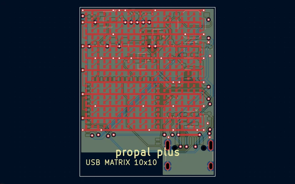
Route a four-layer board and pass DRC
Vector routes the regular parts of the board itself, hands the rest to Freerouting, refills the planes, and runs DRC with schematic parity against your fab’s rules until it comes back clean.
Watch it in Vector