BlogEngineering
Simulate inrush current on a load switch in KiCad with ngspice
Why a P-channel load switch draws an inrush spike, how to simulate it in KiCad’s ngspice, and the gate–drain capacitor fix that cut a 2.47 A spike to 270 mA.
A high-side load switch is a P-channel MOSFET that connects a supply to a load when a microcontroller says so. If the load has a lot of capacitance, the moment the switch turns on, that capacitance charges almost instantly, and the current spike can pull the supply down or trip a USB port’s current limit. You can see this in simulation before a board exists.
The circuit
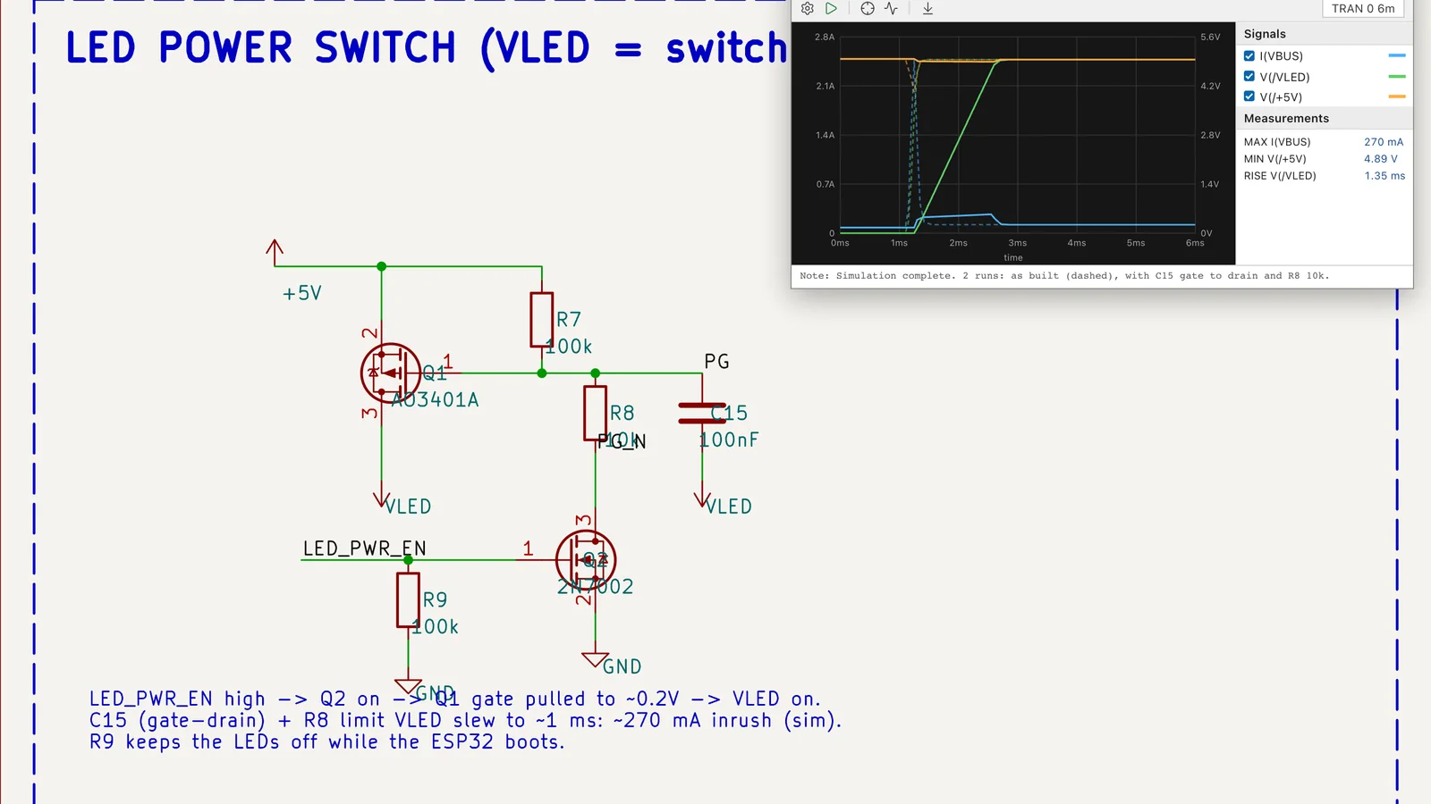
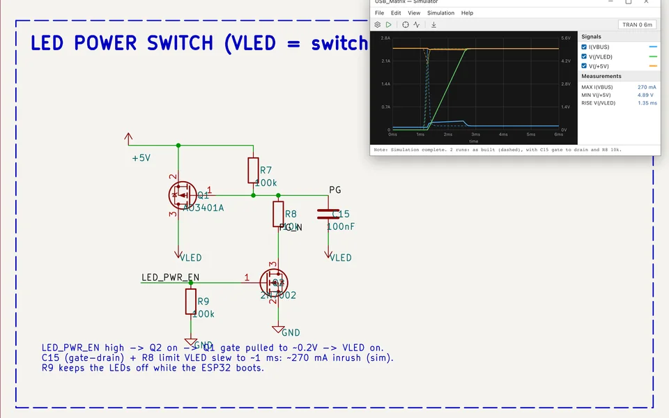
This switch feeds the LED rail on a USB-powered board with 100 addressable LEDs:
- Q1, an AO3401A P-channel MOSFET, from +5 V to the LED rail, VLED.
- R7, 100 kΩ from gate to source, holds Q1 off.
- Q2, a 2N7002, pulls Q1’s gate low through R8, 4.7 kΩ, when the ESP32 drives LED_PWR_EN high.
- C15, 100 nF, from gate to source.
- On VLED: two 22 µF bulk capacitors and seven 100 nF, 44.7 µF in all.
Why it spikes
The current into a capacitor is set by how fast its voltage changes:
I = C × dV/dt
44.7 µF × 5 V / 0.15 ms ≈ 1.5 A on average during the step
With C15 from gate to source, Q1 turns fully on in about 0.15 ms, so VLED steps from 0 to 5 V. The average is 1.5 A; the simulated peak is 2.47 A, and USB 5 V sags to 4.02 V while it lasts.
Simulating it in KiCad
- Give Q1 and Q2 SPICE models from their manufacturers, and set the LED load as a current source or resistor that draws what the LEDs draw when idle.
- Open Inspect → Simulator and add a transient analysis, for example 1 µs steps to 6 ms.
- Drive LED_PWR_EN with a pulse that goes high at 1 ms.
- Probe the current into the supply and the voltages on VLED and +5 V, then run.
The fix: a gate–drain capacitor
Move C15 so it connects Q1’s gate to its drain instead of its source. As VLED rises, C15 pulls the gate with it, so the gate can only move as fast as R8 can charge C15. VLED ramps instead of stepping. Raising R8 slows the ramp further. With R8 at 10 kΩ and Q1’s gate sitting near 1.8 V below the source during the ramp:
I(R8) ≈ (5 V − 1.8 V) / 10 kΩ ≈ 0.32 mA
dV/dt ≈ I(R8) / C15 ≈ 0.32 mA / 100 nF ≈ 3.2 V/ms, about 1.5 ms for 5 V
I ≈ 44.7 µF × 3.7 V/ms + load ≈ 0.17 A + 0.1 A ≈ 0.27 A
| As built | With the fix | |
|---|---|---|
| C15 | Gate to source | Gate to drain |
| R8 | 4.7 kΩ | 10 kΩ |
| Peak supply current | 2.47 A | 270 mA |
| Lowest USB 5 V | 4.02 V | 4.89 V |
| VLED rise | 0.15 ms | 1.35 ms |
The simulated ramp is 1.35 ms, a little faster than the estimate because Q1’s own gate–drain capacitance and the plateau voltage both vary with current. The fix costs nothing: the same capacitor moves, and one resistor changes value.
Vector reads the switch from the schematic, runs the transient in KiCad’s ngspice, edits the circuit in the open Schematic Editor, and reruns it. Watch it on this board.
Questions
- Do I need a separate SPICE program?
- No. KiCad includes ngspice. Assign SPICE models to the parts, open Inspect → Simulator, and run a transient analysis.
- Where do MOSFET models come from?
- From the manufacturer, usually as a .lib or .sub file. Point each symbol’s simulation model fields at it.
- Does the soft start stress the MOSFET?
- It moves the capacitor’s charging energy, about ½CV², into the MOSFET over the ramp. Check that against the safe operating area in its datasheet.
Simulate a load switch before ordering the board
Vector builds a SPICE model from the schematic, runs it in KiCad’s ngspice, changes the circuit in the open editor, and reruns the simulation to show the fix works.
Watch it in Vector