BlogGuides
KiCad to JLCPCB: Gerbers, drill files, BOM, and CPL for assembly
Export everything JLCPCB needs to make and assemble a KiCad board: Gerbers, drill files, a BOM with LCSC numbers, the placement file, and the checks to do first.
To have JLCPCB make and assemble a board, you upload three things: a zip of Gerber and drill files, a bill of materials with LCSC part numbers, and a placement file, which JLCPCB calls the CPL. KiCad can produce all of them. The details that cause trouble are column names, rotations, and parts near the board edge.
What JLCPCB needs
| File | What it is | From KiCad |
|---|---|---|
| Gerbers | One file per copper, mask, paste, and silkscreen layer, plus the outline. | PCB Editor: File → Fabrication Outputs → Gerbers |
| Drill files | Excellon files for plated and non-plated holes. | The Generate Drill Files button in the same dialog |
| BOM | Comment, Designator, Footprint, LCSC, and Quantity for each line. | Schematic Editor: Tools → Generate Bill of Materials |
| CPL | Designator, Mid X, Mid Y, Layer, and Rotation for each part. | PCB Editor: File → Fabrication Outputs → Component Placement |
Add LCSC part numbers
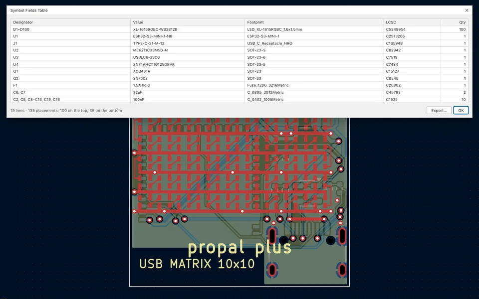
Give each symbol a field named LCSC with JLCPCB’s part number, such as C1525 for a 100 nF 0402 capacitor. The Symbol Fields Table (Tools → Edit Symbol Fields) is the fastest place to fill a column for every part. Prefer basic parts where you can: extended parts carry a setup fee per unique part.
Export the files
The menus work fine. From the command line, the same exports look like this. The BOM command groups identical parts and labels the columns the way JLCPCB expects:
kicad-cli pcb export gerbers -o fab/ board.kicad_pcb
kicad-cli pcb export drill --format excellon --excellon-separate-th --generate-map -o fab/ board.kicad_pcb
kicad-cli sch export bom --fields "Value,Reference,Footprint,LCSC,QUANTITY" \
  --labels "Comment,Designator,Footprint,LCSC,Quantity" \
  --group-by "Value,Footprint,LCSC" --ref-range-delimiter "" -o bom.csv board.kicad_sch
kicad-cli pcb export pos --format csv --units mm --side both -o cpl.csv board.kicad_pcb
KiCad’s placement CSV uses the headers Ref, Val, Package, PosX, PosY, Rot, and Side. Rename them to Designator, Mid X, Mid Y, Rotation, and Layer, and change the side values to Top and Bottom. Then zip the Gerber and drill files together.
Check before you pay
- Rotations and pin 1 in the placement preview. Look closely at LEDs, SOT-23 and SOT-23-5 parts, polarized capacitors, and modules.
- Minimum track, space, via, and hole sizes against the capability you selected. A few 0.09 mm neck-downs can push a board out of the standard process.
- Parts that overhang the board edge. Small boards get edge rails or a panel, and a rail or V-cut on an edge with an overhanging connector won’t work.
- Both-side assembly. If parts are on the bottom, select assembly on both sides, or move them.
An example
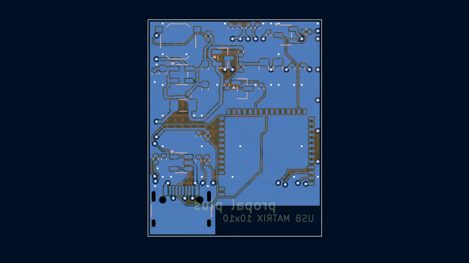
A 27.1 × 33.9 mm, four-layer LED matrix board had 100 LEDs on the top and 35 parts on the bottom. The export came to 11 Gerbers, plated and non-plated drill files, a 19-line BOM, and 135 placements. Its narrowest tracks were 0.095 mm where they necked down at the LED and USB-C pads, so the order used JLCPCB’s 0.09 mm option. The USB-C shell overhung the short edge by about 0.6 mm and the ESP32 antenna by 0.3 mm, so the order asked for rails on the long sides only.
Vector fills in LCSC numbers, exports these files in JLCPCB’s format, and lists what to check on the order page. See it prepare that board.
Questions
- Where do LCSC part numbers go in KiCad?
- In a field on each symbol, usually named LCSC. Fill it in the Symbol Fields Table, and include it as a BOM column.
- Why are my parts rotated wrong in the JLCPCB preview?
- KiCad and JLCPCB define zero rotation differently for some packages. Check every part in the placement preview and correct rotations there or in the CPL file.
- Can JLCPCB assemble both sides?
- Yes, at extra cost. The placement file needs both sides, with a Layer column of Top or Bottom.
Prepare a board for JLCPCB assembly
Vector fills in LCSC part numbers, checks the bottom-side parts and the board edge, and exports Gerbers, drill files, a BOM, and a placement file in the format JLCPCB expects.
Watch it in Vector